



New Delhi: The government has received investment commitments of $11–12 billion under Semicon 2.0, the second phase of India’s semiconductor programme, Union Electronics and Information Technology Minister Ashwini Vaishnaw said on Thursday. The investments are expected to come in over the next two to three years, he added.
Speaking at a press briefing on the sidelines of Semicon India 2026, Vaishnaw said the commitments—“of the order of Rs 1 lakh crore”—covered semiconductor equipment, materials, gases, chemicals, ATMP units, substrates and, in one case, wafers.
He declined to name the companies. “Many of them don’t want us to take the names, so we won’t take the names. They will announce the investments as their boards and their shareholders” decide, he said.
The commitments came alongside a $5 billion investment pledge from Applied Materials, announced earlier in the day. The US equipment maker said the investment, to be spread over a decade under its “India Vision 2035” plan, would support research, supply-chain expansion and workforce development. This includes a new advanced research park and a tenfold increase in its India-based supply-chain capacity.
Semicon 2.0 was approved by the Union Cabinet in July with an outlay of Rs 1,27,500 crore. It is built around six pillars: chip design, machines and materials, fabs, advanced packaging, research and development, and talent.
The first phase, approved in December 2021 with an outlay of Rs 76,000 crore, cleared 12 projects with a cumulative investment of over Rs 1.64 lakh crore. Three have begun commercial production.
Also Read: What it really takes to build an Indian Silicon Valley
Focus of Semicon 2.0 on building ecosystems
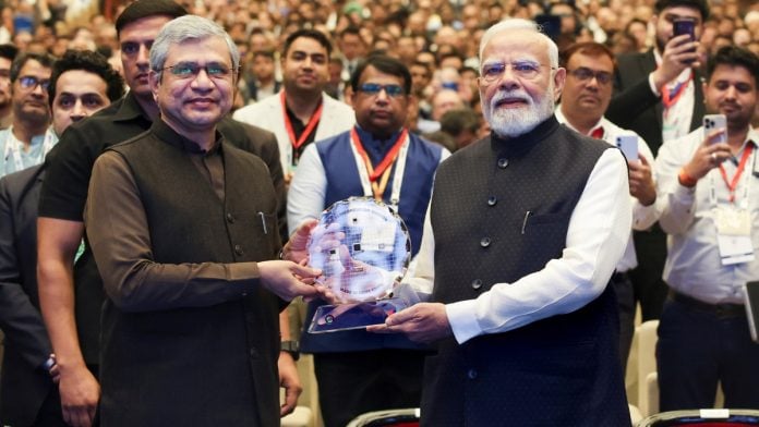
Vaishnaw’s briefing followed the inauguration of the three-day conference at Yashobhoomi in Dwarka by Prime Minister Narendra Modi, under the theme “Silicon to Systems: Building the Ecosystem”. The event has drawn more than 600 companies and delegations from over 50 countries.
Vaishnaw described Semicon 2.0 as a shift from setting up individual factories to building the ecosystem around them. “Semicon 1.0 was all about setting the foundation, making sure that we learn to walk. Semicon 2.0 is more about getting the ecosystem in place,” he said.
On chip design, the first pillar, the government will target at least 200 startups and companies, up from 105 in the first phase. Twenty of the participants secured venture capital (VC) funding totalling around Rs 800 crore.
“We would have been happy even if one or two of them had received VC funding. But 20 of them got it. So that’s why we have kept the target 10x,” he said.
On talent, the sixth pillar, Vaishnaw said the government would train more than 1,00,000 technicians over five years, including clean-room and factory-floor workers, through partnerships with industry and institutes such as Taiwan’s ITRI.
The design programme from Semicon 1.0, which runs across about 400 universities, would also be upgraded to take students from chip design to more complex systems design.
On employment, he said the ecosystem could “very clearly” generate close to one lakh new jobs, calling the estimate conservative.
Asked whether India would adopt an upside-sharing provision similar to the US CHIPS Act, under which the government shares in outsized company revenues, Vaishnaw said programmes had to reflect each country’s circumstances. “US has a very well developed semiconductor industry for many decades… We are starting from practically zero. So every country has to have its own journey,” he said.
A series of agreements was announced alongside the briefing. Tata Electronics signed 16 MoUs spanning the value chain, including one with Ascendas–First Space to develop a 363-acre vendor park around its Dholera fab in Gujarat, and pacts with Fujifilm to localise critical materials and JSR Corporation for photoresists and advanced chemicals.
Other Tata agreements covered wafer manufacturing, assembly and testing with Nexperia B.V., advanced packaging with BESI Singapore, and semiconductor design services with the Semi-Conductor Laboratory.
Other announcements included the exchange of the first batch of commercial devices between Suchi Semicon and eInfochips; packaging tie-ups involving Kaynes Semicon, GridCrest and OptoML; an “Introduction to Semiconductors” course by the India Semiconductor Mission and Intel India; and the establishment of six ChipIN regional centres to expand chip design capabilities across the country.
On the three companies that have begun commercial production, Vaishnaw said their output was already booked and they were competing on quality and cost. He said Micron’s plant had increased its number of tools tenfold since February.
Pressed on yield figures, he said these were company-specific but linked to cost. “If they are competitive on cost, that means they are having good yield,” he said.
Vaishnaw flagged two risks: a disorderly unwinding of accumulated debt in the developed world, which could sour the investment climate, and concentration in global supply chains. “Semiconductor industry is not an easy industry. Had it been easy, then many countries would have done it,” he said.
On where projects would be located, he said the choice rested with industry, based on “policy certainty” and “what kind of support they see from governments”.
(Edited by Chingkheinganbi Mayengbam)
Also Read: Indira Gandhi, Zail Singh and a fire in Mohali—the story of India’s chip dream that almost was