







Semiconductors sit underneath almost every modern system. They run smartphones, cars, hospital equipment, power grids, and defence platforms. The 2021 global chip shortage exposed how much the world depends on a product made in a handful of places, and since then many countries have launched large national programmes to build up their own chip industries, like the US CHIPS Act, and the EU Chips Act. Global chip sales recorded US$795.6 billion in 2025, up 26.2% from 2024. This was driven largely by demand for AI accelerators and memory. Analysts predict sales to head to US$1 trillion in 2026.
For India, chips are a question of national security and industrial policy. The Economic Survey, 2025-26 positions semiconductors as the backbone of energy networks, financial markets, and telecommunications. In December 2021, India approved the first phase of its Semiconductor Mission (ISM 1.0), an outlay of up to Rs. 76,000 crore (about US$9.1 billion). As of July 2026, 12 projects have been approved and several, including Micron, Kaynes, and CG Semi, have begun commercial production. The commitment has since grown further: the Union Cabinet approved a second phase, Semicon 2.0, on 15 July 2026, worth a further Rs. 1.27 lakh crore. However, India’s aspirations in frontier technologies rest on a substrate – semiconductor supply – that the country does not currently control.
To assess whether India’s semiconductor ambitions are structurally sound rather than merely well-funded, it is important to study what subsidies and resource constraints tell us about how realistic India’s targets are – a question of institutional and material capacity.
India’s subsidy architecture for semiconductors
India’s subsidy architecture for semiconductors operates on two tiers, and the logic of each tier is distinct. The central incentive, under the ISM, covers up to 50% of project cost for fabs, compound semiconductor units, and Assembly, Testing, Marking and Packaging (ATMP) or Outsourced Semiconductor Assembly and Test (OSAT) facilities. This design choice reflects a specific theory of risk management: milestone-linked disbursement ties public money to demonstrated progress, reducing the State’s exposure to a project that stalls or fails after receiving support. It also means the central incentive, along with making a marginal site viable, rewards commitment already made rather than generating commitment where none exists.
States add a second tier on top of this, and the pattern across states reveals two different strategic postures. Gujarat contributes a further 40% of the central subsidy amount, a stamp duty waiver, subsidised land of up to 75% on the first 200 acres in Dholera, and power at roughly Rs 2. per unit for 10 years. This is a bundle, combining capital subsidy with reduced land and utility costs, and bundling of this kind functions differently from a flat subsidy by lowering the fixed and recurring costs of operation simultaneously, which compounds an existing advantage. Uttar Pradesh and Tamil Nadu each add 50% of the central incentive as a state top-up, Andhra Pradesh adds 60%, and Odisha adds 50%. These states are pursuing a different logic. Higher percentage top-ups from states with smaller existing industrial bases function as a form of catch-up bidding – an attempt to substitute fiscal generosity for the agglomeration advantages that Gujarat has already begun to accumulate.
The combined effect of these two tiers is substantial. Effective government support for a flagship project can reach 70% to 80% of total project cost once central and state incentives are stacked. This places India’s support scale alongside Japan’s subsidy for TSMC’s Kumamoto fab and ahead of the United States’ CHIPS Act as a share of project cost. A high subsidy share, however, measures fiscal commitment rather than ecosystem depth, and the two are not the same thing. Taiwan, Japan, and South Korea built their manufacturing bases over four decades, accumulating trained workforces, chemical suppliers, and equipment vendors alongside their fabs rather than before them. Although generous subsidies reduce the upfront cost of entry, they cannot shorten the decades needed to develop suppliers, skills, and supporting industries. This distinction explains why NITI Aayog’s own roadmap estimates India will need US$135 to US$180 billion in cumulative investment by 2035 to build a genuinely self-sufficient ecosystem, a figure well beyond the Rs. 76,000 crore ISM 1.0 outlay. The gap between current outlay and this estimate is not a funding shortfall in the ordinary sense. It reflects the difference between subsidising a facility and subsidising an industry, and India’s current commitments are structured closer to the former.
Table 1. State-Level Subsidies and Investment Incentives for the Semiconductor Industry
Source: Authors’ compilation using released State Policies.
Also Read: Bengaluru, Gujarat, Chennai—mapping India’s emerging semiconductor hubs
Four-tier classification of states
Semiconductor ecosystem readiness is not the same as semiconductor ambition. Every state that has published a semiconductor policy wants a fab. States can be grouped into four tiers based on how far each has moved from policy announcement to physical, revenue-generating capacity. The tiering is a ranking of what has actually been cleared, built, or committed.
Tier 1 covers states with an operating or under-construction fab, verified ATMP capacity, and a supply chain that has begun to thicken beyond the anchor projects themselves. Gujarat is the only state in this tier. The Dholera fab is under construction and targets first output by December 2026, and Sanand already hosts three operational ATMP units, run by Micron, Kaynes Semicon, and CG Semi. Two further projects, Crystal Matrix’s integrated compound semiconductor and ATMP facility for Mini and Micro LED displays and Suchi Semicon’s OSAT unit, were approved in Gujarat in a single Cabinet sitting in May 2026. This is the closest India has to the anchor-and-follow pattern that agglomeration theory predicts, where each new project clears less friction than the one before it. Gujarat sits in Tier 1 because its supply chain gap has narrowed, and not because its subsidy is the largest.
Tier 2 covers states with at least one centrally approved ATMP, OSAT, or compound semiconductor project, operating or under construction, but no fab and no independently formed supply chain of their own. As of May 2026, 13 projects, 12 under the ISM and one under the Scheme for Promotion of Manufacturing of Electronic Components and Semiconductors (SPECS), are approved or operational across seven states: Gujarat, Assam, Uttar Pradesh, Odisha, Punjab, Andhra Pradesh, and Rajasthan. Outside Gujarat, this places Assam, Uttar Pradesh, Odisha, Punjab, Andhra Pradesh, Tamil Nadu, and Rajasthan in Tier 2. Assam’s Jagiroad OSAT facility is operational; Odisha hosts India’s first commercial silicon carbide fab, run by SiCSem with the UK’s Clas-SiC Wafer Fab as technology partner, alongside a glass substrate and interposer packaging project from 3D Glass Solutions; and Punjab’s entry is CDIL’s high power discrete semiconductor expansion at Mohali; Rajasthan’s is Sahasra Semiconductors’ ATMP or OSAT facility at Bhiwadi, inaugurated in May 2026 under SPECS rather than the ISM, making it the first semiconductor unit built outside the Mission’s own approval process; Tamil Nadu is India’s largest electronics manufacturing services hub, with Samsung, Foxconn, and Flex already running plants in and around Chennai, and its 2024 policy adds a 50% state top-up on the central incentive, the same rate as Uttar Pradesh. The central government approved two new Electronics Manufacturing Clusters (EMCs) in Manallur and Pillapaikkam worth over Rs. 1,012 crore. Rajasthan’s incentive stack – exemptions on electricity duty, stamp duty, and land conversion charges – mirrors the fiscal logic common to Tier 2 states: compensate for the absence of an existing cluster with lower recurring costs rather than a larger capital subsidy. Each Tier 2 project remains a single, standalone facility. None has yet triggered a second or third investor the way Sanand did in Gujarat.
Tier 3 covers states with a dedicated semiconductor policy and a genuine supply chain or design ecosystem, but no centrally approved manufacturing project of their own. Karnataka is the clearest case, and is conspicuous by its absence from the approved project list even though it brings something no Tier 2 state has. Karnataka is India’s design capital, home to the bulk of the chip design and verification talent, and its Electronics System Design and Manufacturing (ESDM) policy offers a 10% capital subsidy alongside R&D grants and patent reimbursement. What separates Tier 3 from Tier 2 is not incentive generosity. It is that neither state has converted its underlying strength – design talent in the case of Karnataka – into an ISM approved fab, ATMP, or compound semiconductor unit.
Karnataka has signalled bids for a second silicon fab, alongside Uttar Pradesh and Maharashtra, and either would move directly into Tier 1 or Tier 2 the moment a central approval comes through, since the ecosystem gap that usually slows a new entrant is already smaller in these states than elsewhere.
Tier 4 covers states with a state government approval or memorandum of understanding for a fab, but no central clearance and no operating facility. Maharashtra is the example. Its cabinet approved a US$10 billion fab proposed by the Adani Group and Israel’s Tower Semiconductor at Taloja, Panvel, in September 2024, with a stated first phase capacity of 40,000 wafers a month. The project never received ISM approval, and by September 2025 Adani had ended its partnership with Tower and was searching for a new technology partner, with the state government issuing a comfort letter allowing the allotted land to be repurposed for a data centre if no semiconductor partner materialises. Maharashtra illustrates why a state cabinet approval and a central ISM approval are not interchangeable. A state can approve land, tax breaks, and a headline investment figure unilaterally. It cannot approve technology transfer, and it cannot compel a foreign partner to remain in a joint venture. Tier 4 projects therefore carry a risk that Tier 1 and Tier 2 projects do not: the headline investment figure can collapse without any policy failure on the state’s part, simply because the private partnership underneath it did.
Table 2. Classification of Indian States by Semiconductor Project Status and Ecosystem Readiness
Source: Authors’ analysis using policy trackers and updates.
Figure 1. Tier-wise semiconductor ecosystem readiness across Indian states
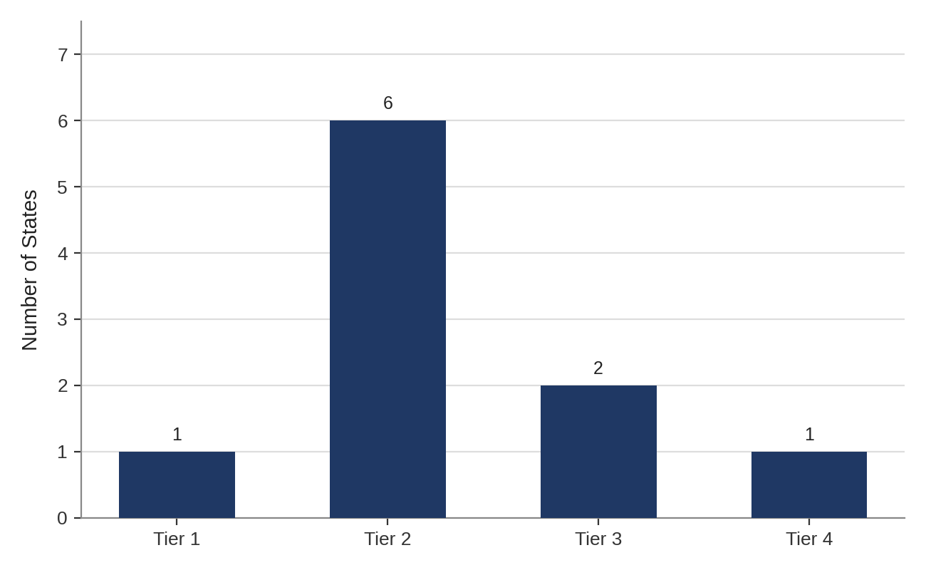
Figure 2. Semiconductor project distribution by tier
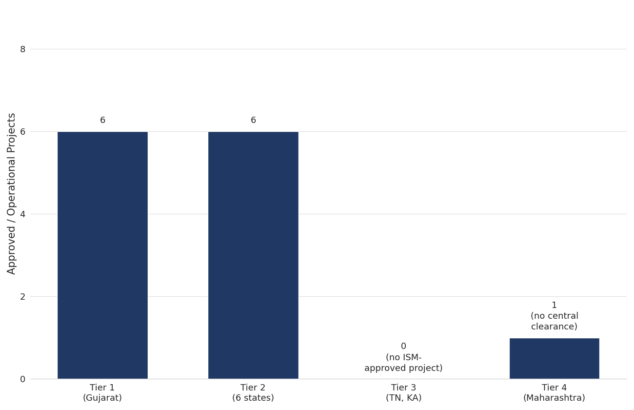
Why some tiers are better than others follows from the following discussion. Tier 1 status reflects a state that has already paid the fixed cost of assembling pre-cleared land, reliable power, treated water, and a forming supply chain, so each additional rupee of investment faces less friction than in a state starting from zero. Tier 2 states have proven they can clear the lower bar of an ATMP or OSAT unit, which needs far less water and power than a fab, but none has yet demonstrated the harder capability of hosting fabrication itself. Tier 3 states hold a structural advantage, design talent or manufacturing depth, that has not yet been tested against the ISM’s own approval process, so their readiness is real but unproven at the fab or ATMP stage. Tier 4 exposes the ceiling of what a state government can unilaterally guarantee: land and fiscal incentives, but not a technology partner’s continued commercial interest. The practical implication is that state tiering should track physical and contractual milestones, land in hand, power and water infrastructure commissioned, a central ISM or SPECS approval secured, first output achieved – rather than the subsidy headline, because subsidy size has repeatedly proven a poor predictor of which projects actually get built.
Table 3. Water Management Capacity and Constraints across Indian Semiconductor States
Source: Authors’ compilation using NITI Aayog Composite Water Management Index reporting 2.0 (2019, last released version).
Conclusion
India’s semiconductor programme has resulted in significant financial commitment. There are two levels of subsidy: a central incentive that can cover half of the project cost, and state top-ups that increase effective support to 70-80 % of the project cost. However, the evidence across states shows that project attraction and ecosystem creation are not the same. The four-tier paradigm presented in this analysis demonstrates that budgetary commitment and ecosystem preparation have progressed at different rates. Gujarat alone has begun to turn subsidies into the anchor-and-follow pattern predicted by agglomeration theory, with a fab under development and three functioning ATMP units attracting new entrants such as Crystal Matrix and Suchi Semicon. Each of the seven Tier 2 states hosts a single standalone facility, and Karnataka carries design and manufacturing depth that remains untested against the ISM’s own approval process. Maharashtra’s stalled fab shows the limits of a state cabinet approval, since it cannot compel a private partner to remain in a joint venture once commercial interests fade. The gap between the Rs. 76,000 crore committed under ISM 1.0 and the further Rs. 1.27 lakh crore approved under Semicon 2.0, and the US$135 to US$180 billion that NITI Aayog estimates India may need by 2035, shows how much work remains, building suppliers, training a workforce, and securing water and power infrastructure at scale. India has purchased its way to the forefront of the semiconductor sector. Converting that position into a long-term ecosystem will require a decade of state-level execution, in which land, water, and electricity infrastructure is developed and tested against demand.
Dr Srishti Gupta is an Assistant Professor in the Tata Chair Unit at the Institute of Economic Growth (IEG). She tweets @DrSrishtiG02. Kushal Kabra is pursuing a B.A. (Hons) in Economics from Shri RamCollege of Commerce, University of Delhi.
Views are personal.
This article was originally published on the Ideas for India website.