


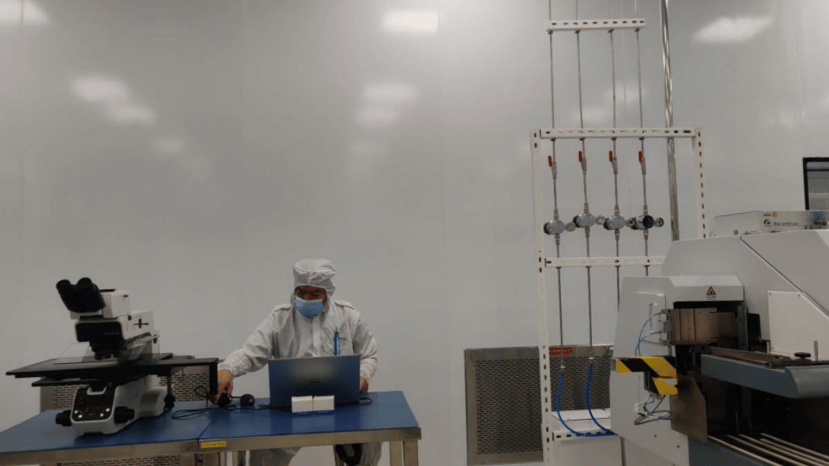
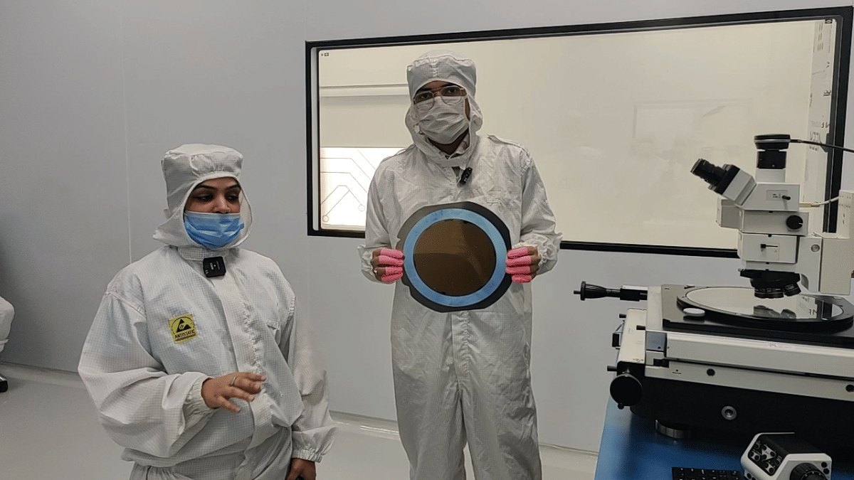
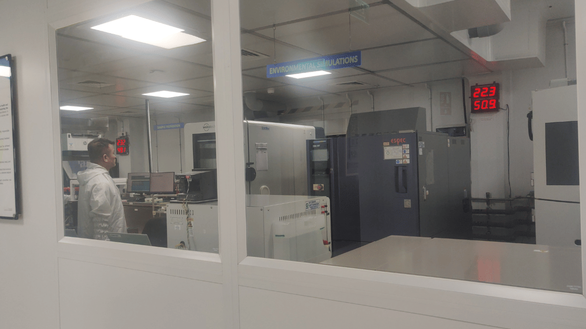
Sanand (Gujarat): It’s about 47 degrees outside. Inside, it feels 20. Deepa Jayasri, a recent electronics engineering graduate from LDRP Institute of Technology and Research College in Gandhinagar, is dressed head to toe in a white anti-static gown, cap, and shoe covers—looking less like a factory worker and more like someone about to perform surgery.
The 23-year-old is bent over an inspection station inside the Kaynes Semicon facility in Sanand, measuring the thickness of a bond line on a chip the size of a fingernail, cross-referencing the number against a specification sheet on her tablet.
The bond line is the width of the point where a wire connects to the chip, a critical quality measure. Deepa has been working here for eight months. Before that, she had never seen the inside of a semiconductor facility. Neither had most of her colleagues.
The room is silent except for the hum of the air filtration systems.
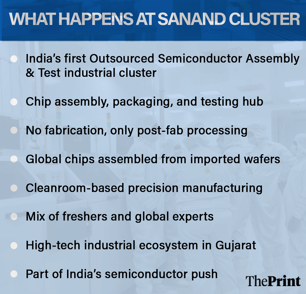
This is the Kaynes Semicon’s Outsourced Semiconductor Assembly and Test—OSAT— facility, where chips that go into air conditioners, washing machines, electric vehicles, and refrigerators are packaged and tested before being shipped to the US, and beyond.
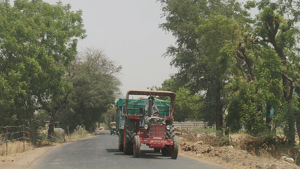
It’s one of three such facilities now operational in the Sanand Gujarat Industrial Development Corporation (GIDC) cluster, 30 kilometres from Ahmedabad. Together, they represent something India has never had before: semiconductor packaging and testing capacity at industrial scale.
The anti-static gown Deepa wears is not a uniform choice. Static electricity—the mild charge the human body builds up by walking across a carpet—can permanently destroy a chip worth hundreds of dollars. The gown continuously drains that charge.
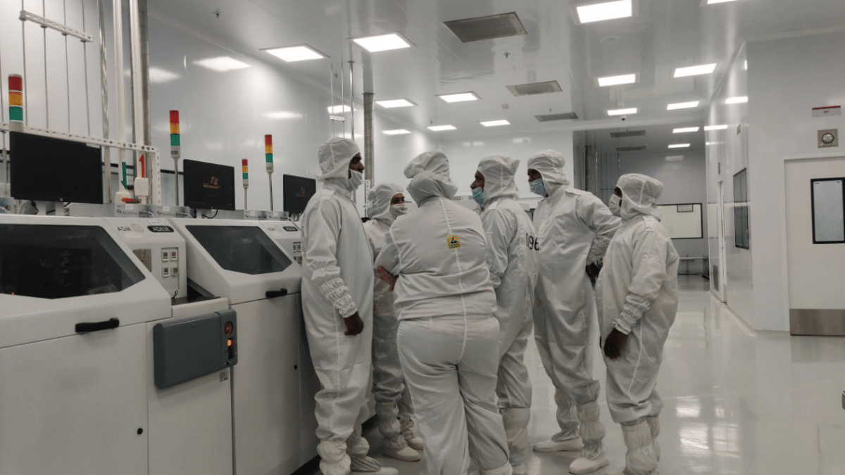
Inside the cleanroom, air pressure is kept slightly higher than outside so that any breach causes air to flow outward, keeping contaminants out. The floor is divided into cleanliness zones—10,000 and 100,000 allowable airborne particles per cubic foot. In the more controlled zone, a fleck of dust invisible to the human eye is large enough to ruin a chip.
Beside Deepa, on the same floor, are veterans from Malaysia and the Philippines who have spent careers in the OSAT industry—a global business dominated for decades by Southeast Asian countries, where India is now making its first serious entry.
Also Read: Why India’s manufacturing-first approach to semiconductors is unsustainable
What actually happens at these facilities
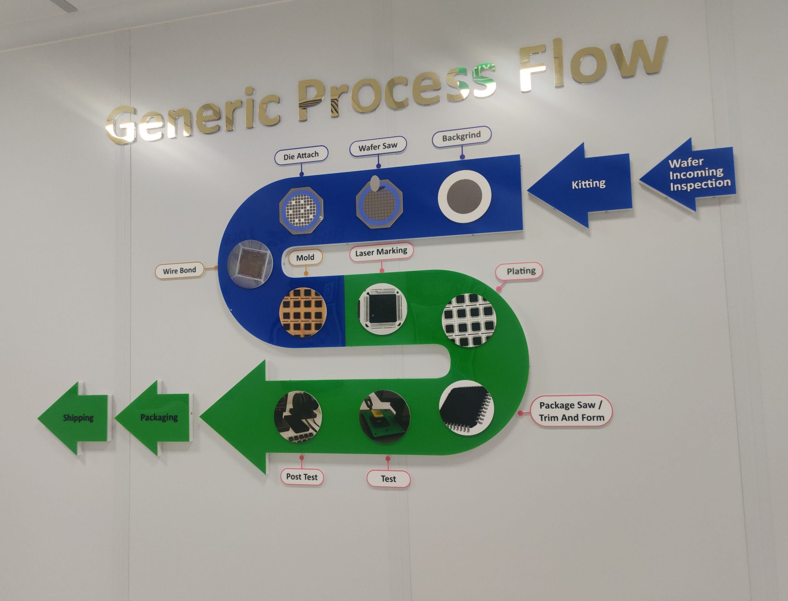
A semiconductor chip goes from blueprint to device in five broad stages: design, fabrication, packaging, testing, and shipping.
Design is where engineers create the blueprint of a chip—what it will do and how its circuits will be arranged. Fabrication is where those blueprints are physically etched onto silicon wafers using light and chemicals inside highly specialised plants called fabs.
Packaging is where the wafer is cut into individual chips, each mounted onto a metal frame and encased in a protective shell. Testing is where every chip is electrically verified before it leaves. Shipping is where the finished chip enters the global supply chain and ends up inside a device.
India has designed semiconductor chips for global companies for three decades. Around 30 percent of the world’s chip designers are Indians, and roughly 20 percent of a chip’s components get designed here—at India offices of Qualcomm, Intel, AMD, and others.
The intellectual property rights, however, rest with those foreign firms, and fabrication, packaging, and testing have happened entirely abroad—fabricated in Taiwan, packaged in Malaysia or the Philippines, tested in Thailand.
What Sanand is now attempting, for the first time, is to bring the packaging and testing stages to India. What Sanand does not yet have is chip fabrication. That requires a fab costing billions of dollars and years of construction. Tata Electronics is building one in nearby Dholera, targeted for production around 2028-29.
The three Sanand facilities receive wafers already fabricated abroad and take over from there—cutting, packaging, and testing every chip before it is shipped.
The three facilities make three different types of chips.
Kaynes makes Intelligent Power Modules, or IPMs—chips that control electrical flow in motors and appliances, used in ACs, washing machines, EVs, and industrial drives.
CG Semi, a joint venture between India’s CG Power and Japan’s Renesas Electronics, makes logic chips for consumer electronics and automotive systems. Logic chips control and process functions inside devices and vehicles, and do not act as memory storage or power supply chips.
Micron Technology, headquartered in Boise in the United States, makes memory chips for its own global supply chain.
Of the 12 semiconductor projects approved under the Centre’s India Semiconductor Mission Gujarat hosts four, three in Sanand and one in Dholera.
Kaynes CEO Raghu Panicker traces the consumer impact plainly. The power module inside a split AC is currently imported. When Kaynes makes it in India, the chip cost falls, the module cost falls, and so does the price of the split AC, eventually. “We are doing IPM products in our factory. The same IPM products will go to the air conditioners. Thereby, the air conditioners price has to come down. This will all happen. It has just begun.”
When ThePrint spoke to the sarpanch of one of the villages bordering the cluster, he did not talk about India’s chip ambitions or the Prime Minister’s visits. He talked about salaries.
“If a family has five members, at least one of them is working in some company,” he said. “Rs 10,000-15,000 coming in, that is a good system.” That arithmetic sits alongside the larger numbers—and, in its own way, is just as telling.
Step by step, chip by chip
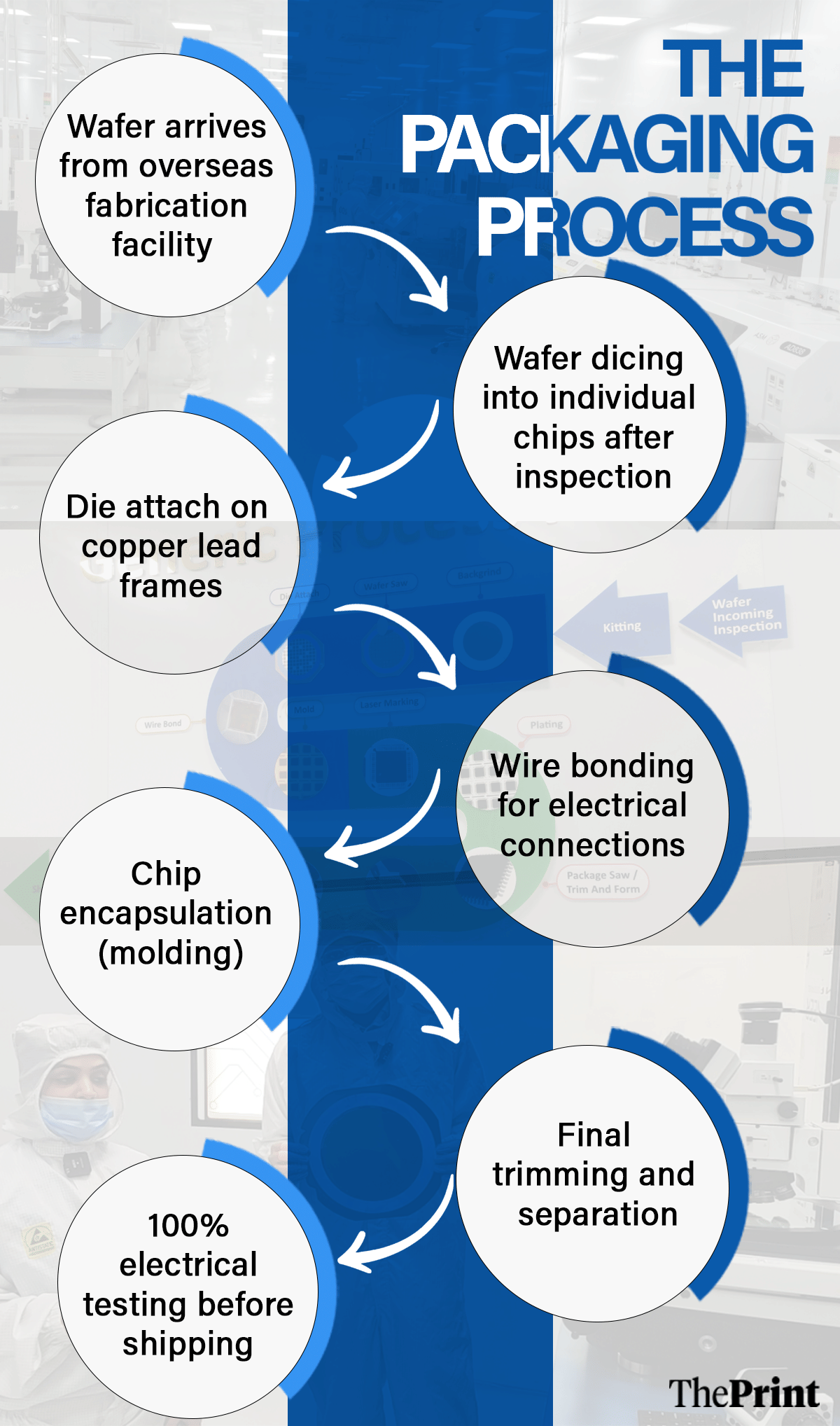
The production process at Kaynes runs through seven to eight steps. A silicon wafer, roughly the diameter of a dinner plate and thinner than a fingernail, arrives from a fab abroad, carrying hundreds of microscopic circuits already etched into its surface.
Each circuit is one chip. The job of the OSAT is to turn that disc into individual packaged chips that can survive the real world.
Suman Mondal, a graduate of Swami Vivekananda Institute of Science and Technology, works on incoming quality control—the first gate everything passes through.
Every batch of wafers, lead frames—a thin metal structure that holds and connects the semiconductor chip to the outside world—and solder paste is measured and verified before it touches anything else. If exposed to oxygen, silicon wafers oxidise and become unusable, so they go immediately into sealed nitrogen cabinets.
If something defective slips through at this stage, it will not be caught until the final testing stage at the other end of the line, by which point every step in between will have been wasted, and a faulty chip could end up in a customer’s hands.
The stakes of this seemingly routine checking, Suman says, are anything but routine.
Tanya Shah, also from LDRP, works at the dicing station, where a diamond-blade saw cuts the wafer into individual chips at tolerances measured in microns—one micron being one-seventieth the width of a human hair.
She applied for the Kaynes training programme without fully understanding what an OSAT was. “Because of Kaynes only, I have come here. They have given a course of 10 weeks in which we have learnt what the OSAT is. After going through that whole course, we got to know that it is a good opportunity for a fresher.”
From dicing, each chip is bonded onto a copper lead frame using solder paste—the die attach stage—and then goes through a reflow oven where the paste liquefies and solidifies into a permanent joint.
Then comes wire bonding: a machine picks up a wire thinner than a human hair and attaches one end to a contact inside the chip and the other to the lead frame, creating the electrical bridge that allows the chip to communicate with the outside world.
It does this repeatedly, at speeds that appear to the naked eye as a continuous blur. A single broken wire renders the chip dead.
Ritesh Ram, from Government Polytechnic, Diu, manages the molding station. At this point in the process, the chip—with all its microscopic wire connections exposed—is entirely vulnerable to heat, moisture, and physical contact. His machine encases the entire assembly in a hardened polymer compound, pressing it under heat and pressure until it sets into the hard, flat black rectangle that most people recognise as a chip. It is the chip’s armour.
“Without molding, the chip cannot survive in an external heat and moisture environment,” Ritesh says.
After molding, Kishan Gupta from LJ College handles trimming and singulation—cutting the lead frame apart into individual packaged chips, their metal leads electroplated against corrosion.
Testing is where everything comes together, or falls apart.
Paul Ilanghopan, Head of Operations at Kaynes, who built his career across Southeast Asia’s semiconductor industry, oversees this stage alongside Ravi Sagaravan, who came from Malaysia to lead the testing operation.
Every chip—not a sample, every single one—is tested electrically. The tester sends precisely defined signals into the chip and measures whether the response matches the design specification exactly.
Chips that pass go into final packaging—tape reels, trays, vacuum-sealed tubes. Chips that fail are binned. Nothing defective leaves the building. Kaynes currently has over 130 employees, including more than 20 freshers, with the rest bringing prior industry experience.
A melting pot—in a dry state
Nanie Torres, the General Manager of the Kaynes factory, came from the Philippines. Paul came from Chennai. Ravi came from Malaysia. Azni, also part of the Kaynes team, came from Malaysia. Together with senior managers from Japan and other parts of the region, they form the international layer of a workforce where the freshers are now, by Torres’ reckoning, somewhere between level two and three on a scale of 10.
That sounds modest until she adds, “They’re the ones actually, in some cases, explaining to our customers, to our partners.” A fresher from Bihar, eight months into her first job, is walking a customer engineer from the United States through an inspection process.
The plan is to expand the fresher intake from the current 20-plus to between 45 and 90 in the next phase, while the expat headcount, currently 25 to 30, grows more modestly before eventually reducing as Indian engineers develop the depth to take over. “We cross-pollinate from whatever is the local and whatever is the foreigner, the international that we are currently bringing,” Torres says.
Azni describes his days in Sanand with the matter-of-factness of someone who has relocated for work across multiple countries. “We are more focused on technical manufacturing and operation. To us, it is not a big deal—we come from where we stay, then we just go to the factory and then we just work on it. By the time we finish, it is very late in the evening.”
Paul raises one practical gap the international team has flagged to the state government: Gujarat is a dry state, and hosting customers and vendors over dinner, routine in Penang or Laguna, creates a limitation that does not exist in any of the Southeast Asian OSAT hubs these engineers came from.
“We have already highlighted this to the government. Because that kind of thing is needed for any business.” A pause. “But we are okay. We don’t drink.”
Why Gujarat
When semiconductor companies were evaluating Indian states, the deciding factor was not the headline subsidy figure. It was certainty.
Gujarat State Electronics Mission (GSEM) published a single transparent policy in 2022, applying equally to every investor. Tata’s one-lakh-crore fab and CG Semi’s OSAT get the same terms, in writing, publicly available. “Be it Tata, be it CG, be it an American giant called Micron, they are all getting the same benefits,” a senior GSEM official told ThePrint. “It is not a closed door decision between any politician and any company CEO.”
A senior CG Semi official, speaking on the condition of anonymity, said the company modelled a one-year lag for subsidy disbursement—standard caution for large projects in India. “We got it in one month. Imagine the level of efficiency.”
The official adds that all government relations were handled without paying a bribe. “I have not paid a single rupee to any officer at any level and I have got everything done.”
Every 15 days, a coordination meeting brings all relevant government department heads together with the companies to resolve problems on the spot. “What corporates hate the most is uncertainty,” the official says. “I have faced zero of that problem.”
On power and water, Gujarat has surprised even sceptics. Certain machines auto-shutdown if voltage dips for even a few milliseconds; the state has committed to 24×7 uninterrupted supply and companies say it is delivering.
When a representative from JICA—Japan International Cooperation Agency, which funds infrastructure and industrial projects across Asia—came to evaluate a potential investment and was told water was not a problem, they did not believe it. They triple-checked, hired a verification company, and spoke to villagers. Supply, they confirmed, was continuous.
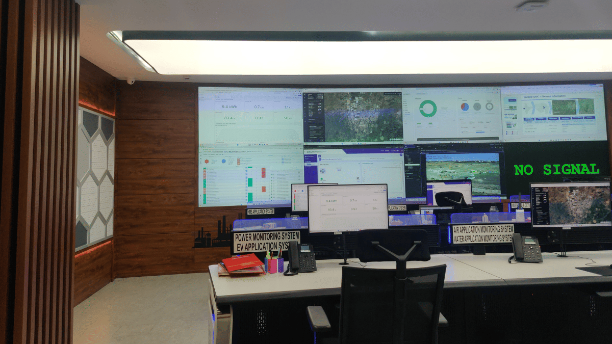
Command & control centre, and its complaints
The Sanand GIDC covers 2,000 hectares across a 90-kilometre perimeter, monitored from a single room: the command and control centre. Nine CCTV points cover the estate. Smart water meters on every industrial plot alert the centre the moment consumption crosses its permissible limit.
Complaints arrive via WhatsApp and are reviewed weekly. The range is wide. During the last monsoon, Micron complained about a mosquito problem at the facility, directly to the Prime Minister’s Office (PMO). “These are the kind of things that GIDC officials also have to handle,” the GIDC official told ThePrint, without evident irony.
Food courts and a business park are being developed within 500 metres of the semiconductor facilities. Multi-storey migrant worker housing is under construction for the thousands of workers arriving from other states.
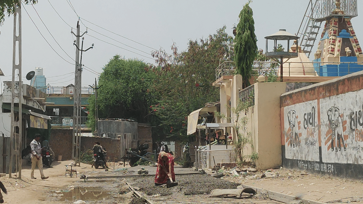
Not everyone in the surrounding villages is satisfied, though. ThePrint spoke to several residents, who spoke in Gujarati, with responses later translated.

Parshuraman Patel, a shopkeeper near the cluster, said water has become noticeably harder since the industries came in, and has worsened since Micron, one of the highest water consumers in the cluster, became operational.
Semiconductor manufacturing requires vast quantities of ultra-pure water, processed through multiple filtration and chemical treatment stages.
This large-scale extraction can affect the mineral balance of groundwater in surrounding areas, turning into hard water—meaning it contains higher levels of dissolved minerals such as calcium and magnesium, which affects taste, causes scale buildup in pipes, and makes the water feel different for daily use.
Maniyaben, who works on a construction site at one of the facilities, said the deterioration had become a recurring concern among women in the area who manage household water use.
The GIDC official acknowledged the complaints but maintained the cluster draws from a separately allocated supply and does not affect drinking water availability for surrounding villages. The question of quality, as opposed to quantity, remains alive.
Bol village, which borders the cluster, has one of the highest girl dropout rates in the district.
CG Semi: a different model
While Kaynes recruits engineering graduates from colleges across India, CG Semi has drawn its operator workforce, the people who physically run the machines, from tribal areas of Chhattisgarh and Jharkhand. The engineers at CG Semi come from Indian universities, including Gujarat colleges and NITs.
Every operator on the CG Semi floor right now is a woman.
For many, it is the first time they have lived outside their village. CG Semi is building dedicated accommodation on the estate. “We cannot expect them to find their own accommodation. It would be their first days outside the villages,” a senior CG Semi official, speaking on condition of anonymity, told ThePrint.
Before going on the floor, both engineers and operators were sent to Renesas’ facility in Malaysia for three months of training. They came back and ran the machines independently.
Renesas recently conducted a full process quality audit of the Sanand facility. In the global OSAT industry, 80 percent is considered good. CG Semi scored 92. “Which means our quality is even better than many of the well-established OSATs globally,” the CG Semi official said. “That was our entire objective in getting the expats, because we have actually hit the ground running on quality.”
Every machine in the facility is the global best-in-class for its category. The backup power system runs on maglev (magnetic levitation) technology, the same principle that powers bullet trains: rather than mechanical parts in contact, the system floats on magnetic force, making it more stable, more reliable, and less power-hungry than the conventional systems used by 90 percent of the industry.
The facility also has an in-house electroplating line, which most competitors outsource. Once a customer qualifies a supplier in this industry—a six-to-nine month process of rigorous technical scrutiny—they almost never switch. The 92 percent audit score exists to make that decision straightforward before a customer even raises a question.
The stakes
India has zero history of semiconductor manufacturing. Not a modest one—zero.
The GSEM official is direct: this is the first time a semiconductor facility is being established in a developing nation, with companies simultaneously betting on India’s utilities, workforce, and administration. If the projects fail, the damage extends far beyond Gujarat.
“The entire world is watching very intently,” he said. A failure here will be remembered for a decade. A success will bring SK Hynix, Kioxia, and every global player that has so far held back.
Inside the Sanand cluster, that ecosystem is already forming—in the food courts near Micron’s gate, in the migrant housing for workers from tribal Jharkhand, in the command and control centre fielding complaints that reach the PMO. And on the production floor, where Deepa Jayasri, in her white anti-static gown, is explaining an inspection process to a customer from the United States. Eight months ago, she did not know what an OSAT was.
(Edited by Ajeet Tiwari)
Also Read: India plans $10.8 billion fund to support local semiconductor manufacturing